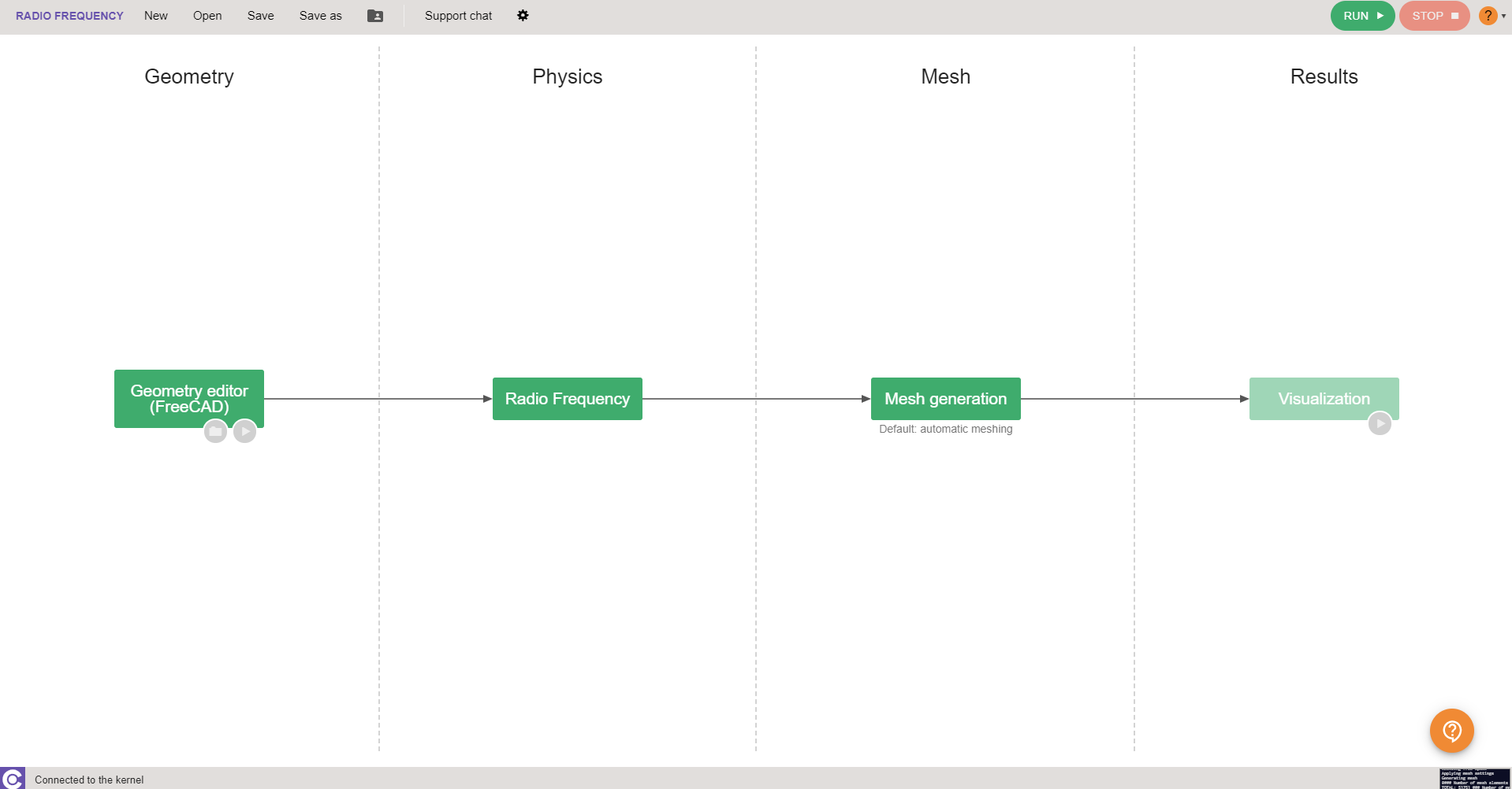
Patch antenna simulation setup
PCB/planar/patch antennas are very widely used in modern electronics, and often it is beneficial to make a computer model to predict the behaviour of the patch antenna even before the physical tests have started.
In this guide we will take a look at how to build a complete patch antenna simulation from scratch in CENOS Radio Frequency app, using its built-in geometry editor, FreeCAD.
Case setup
Before we can actually start building our simulation, we need to first prepare our case - choose the way we will build our geometry, and save the case.
Choose geometry approach
You have three options from which to choose - Templates, Import CAD (if you have your own CAD file ready) and Geometry Editor.
Patch antenna can be simulated with any one of these approaches, as there is also a template for it, but for this example we will choose Geometry Editor and build our patch geometry ourselves.
Save the case
At this point you need to save the case, otherwise if you try to open FreeCAD, CENOS will not let you move forward.

Once the case is saved, click the Play icon to open FreeCAD - CENOS geometry editor.

Geometry creation
In FreeCAD we have all the possibilities to build our antenna geometry, and we are going to do just that.
In this Geometry creation section we will cover all main points you need to complete to build your own patch antenna geometry manually.
Substrate (dielectric)
First thing we need to do is to build the substrate. The easiest way to do that is through box creation.
In Part workbench create a box and change the parameters to the values corresponding to your antenna substrate.

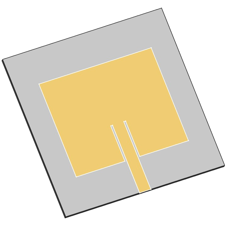
Patch / Conductive layers
Next we need to create the patch for our antenna. In Sketch workbench patch can be drawn directly on the substrate as a 2D sketch or created as a 3D extrusion. They both work!
PROS/CONS
For 2D patch:
- Easier to create (Sketch on surface).
- Can avoid meshing problems.
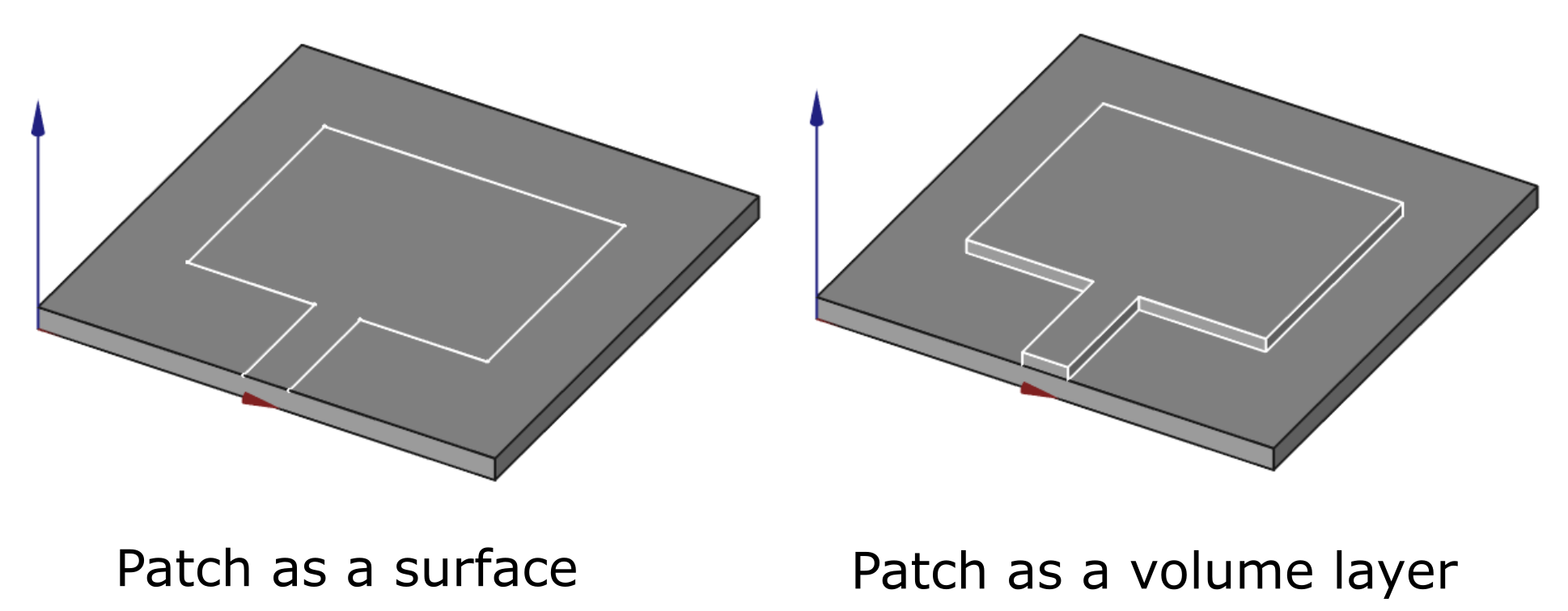
For 3D layer:
- Slightly more difficult to create (Have to create an extrusion).
- More accurate results.
Feed networks
For more complex patch antennas the feed network needs to be drawn separately. To make the feed creation as fast and easy as possible, CENOS has a specific tool designed for this exact purpose.
In Sketch workbench create a sketch on top of the substrate volume.
Create the feed lines as 1D edges.
Create the patch surfaces as fully closed wires.
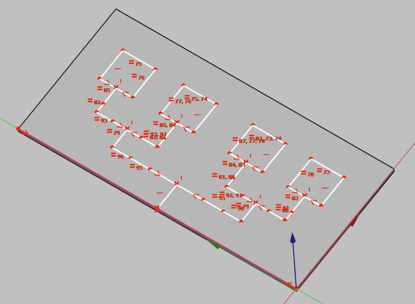
Close the sketch, switch to Part workbench and select the sketch object.
Select the Feed Network tool

Select all edges with the same trace width and click Add to create separate width groups for each of them.
- Create one group with a width of 0 for the all of the *enclosed patch edges.
- Click OK to generate the feed network.
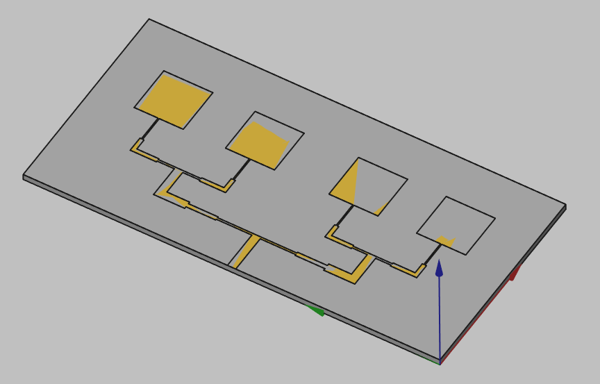
note
You will see some visual artifacts (the golden feed surface will appear to flicker). This happens when two surfaces overlap, this is normal behavior and means you did everything correctly!
tip
You can create chamfered corners by filleting the sketch path with a radius half of the trace width:

Send geometry to CENOS
Once you have finished the geometry, you need to send the mesh to CENOS. To do that:
Select all final objects in the tree view.
Click Geometry to CENOS.
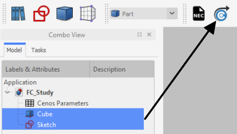
As geometry is being sent to CENOS, FreeCAD study will be automatically saved in the simulation folder, so you can close it.
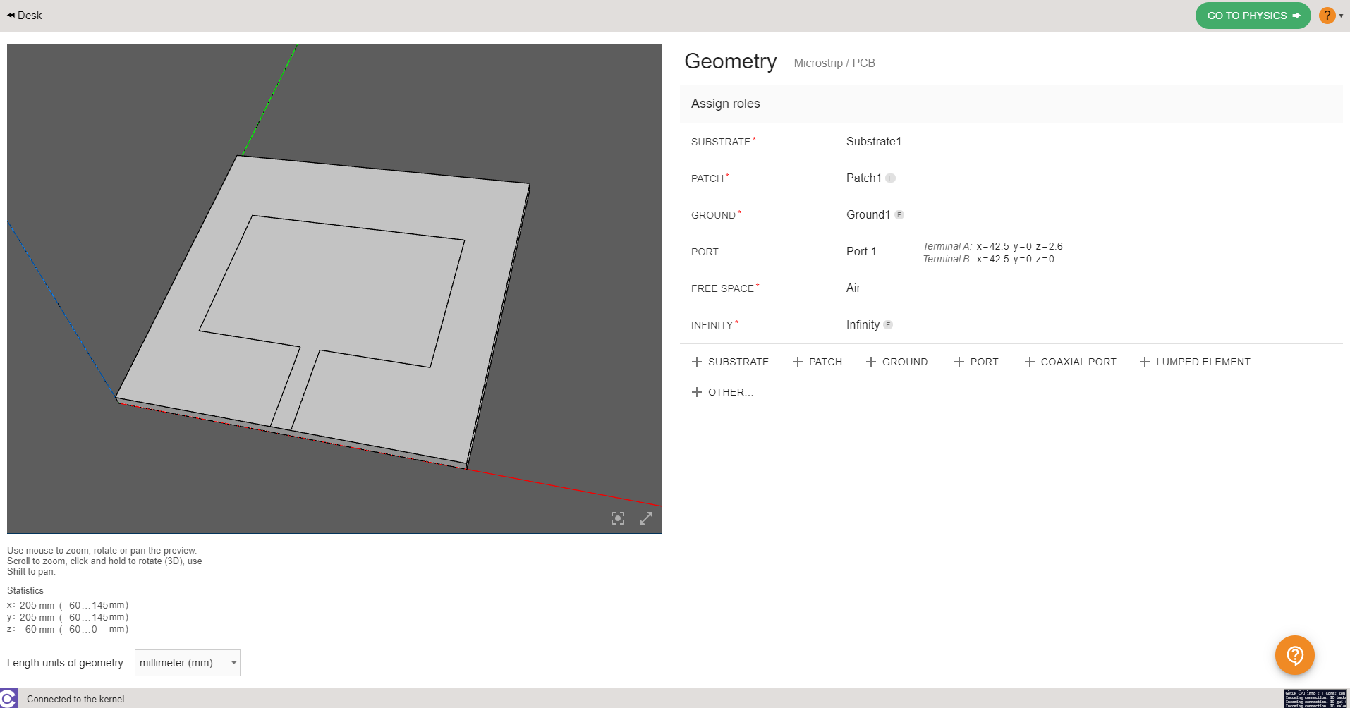
Roles
Once the geometry is finished and sent to CENOS, you need to define your geometry before defining the physics on it.
Essentially you need to clarify which part of your geometry is the dielectric, which is the port etc., in other words, define roles for parts of your geometry.
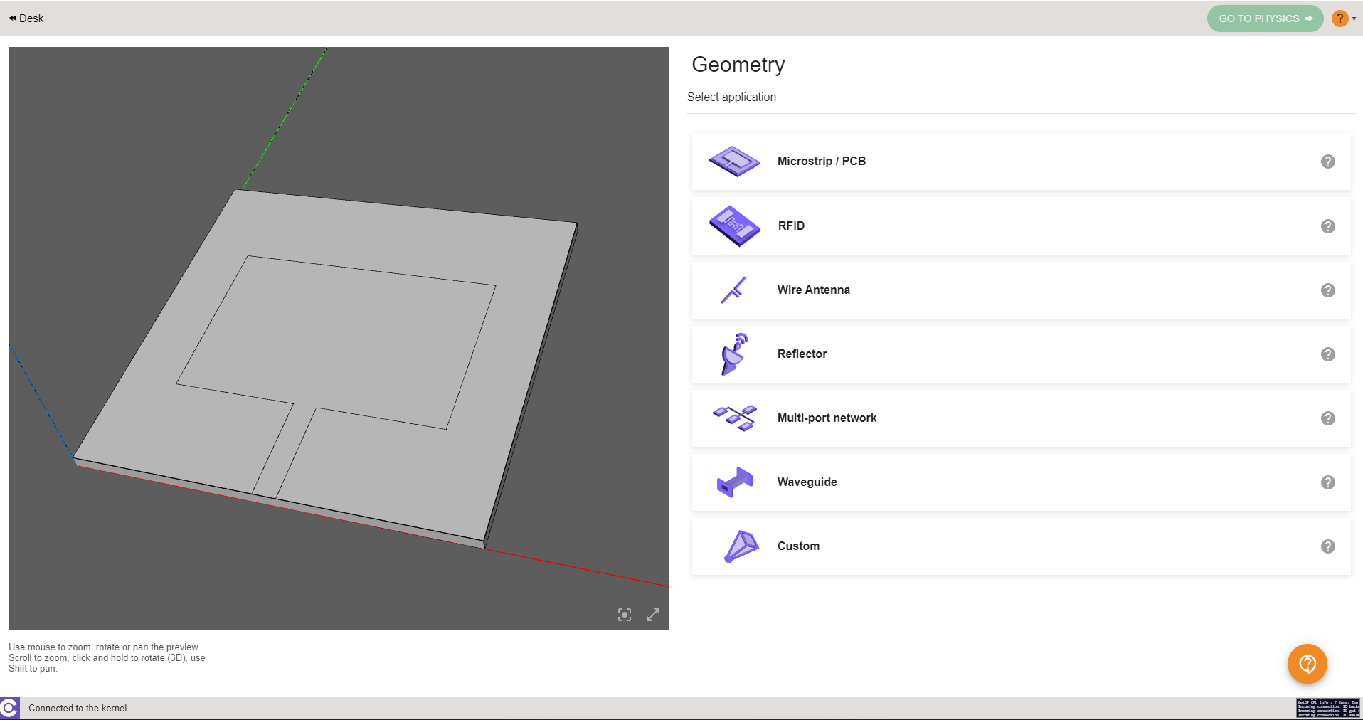
Type of antenna
Before you define roles, you need to select what kind of antenna you have - Microstrip, RFID, Wire, Reflector, Multi-port network, Waveguide or Other.
For this example we choose Microstrip/PCB antenna type.
Surface/volume roles
Now you need to define surface and volume roles for your substrate, patch, ground and port.
Got to physics
When roles are assigned, GO TO PHYSICS button will become active - click it to move to the Physics definition!

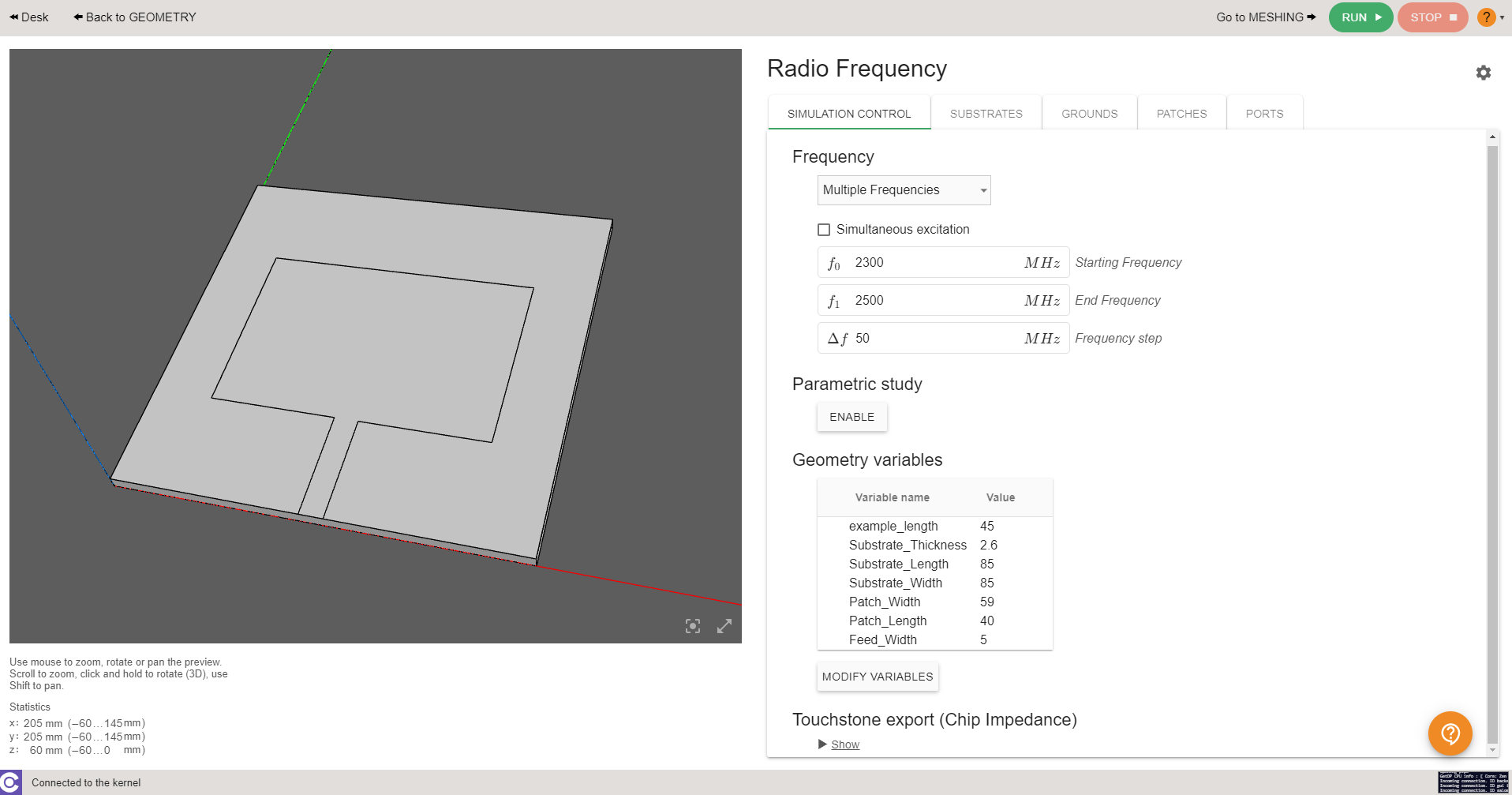
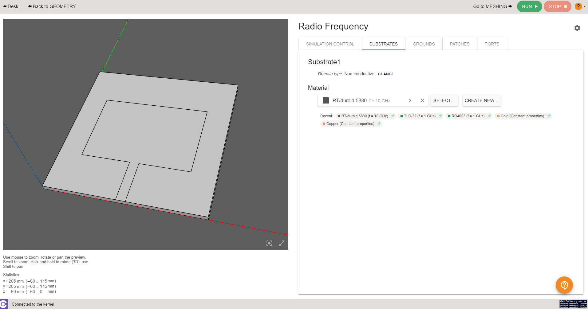
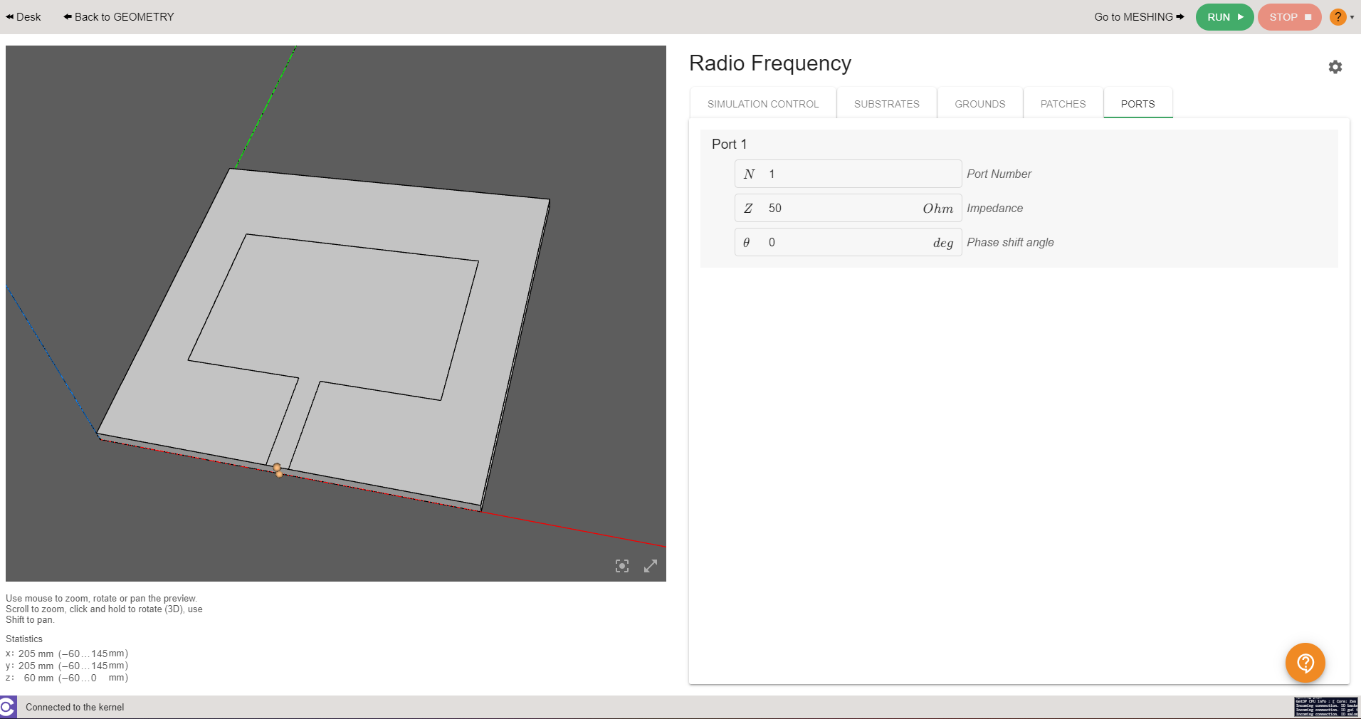
Physics
In physics you need to define the physical parameters of your simulation, which include frequencies, material definitions and boundary conditions.
Simulation control
In SIMULATION CONTROL you define either a single frequency or a frequency sweep.
Volumes
For substrate you only need to specify the material.
Boundaries
Boundaries or boundary conditions have also been predefined:
Uniform Port → Default 50 Ohm Impedance.
Patch and Ground → Perfect Electric Conductor.
Once all physical parameters are filled, RUN button will become active and you will be able to run the simulation!

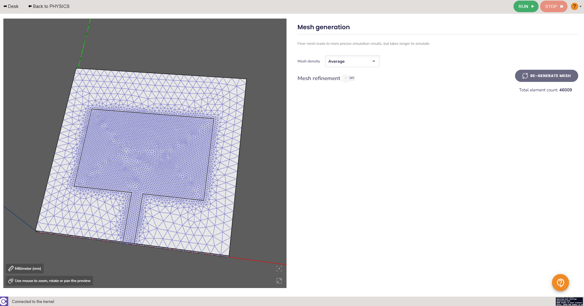
Manual meshing
If during the calculation you get a message about meshing problems, you will need to manually mesh your antenna. You can also mesh it manually already in the mesh generation section in case you want more control over your simulation.
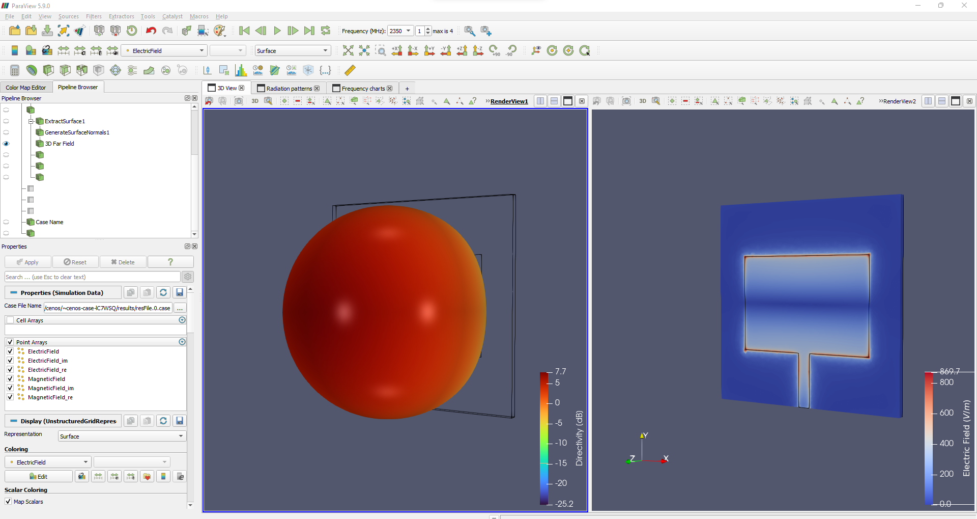
Results
When calculation is done, results will automatically open in a new window. Congratulations, you have successfully finished a patch antenna simulation!